Spectroscopic ellipsometry
Ellipsometry is a non-destructive method for analyzing optical constants of bulk materials and thin films. In the case of thin layers, it can determine the thickness of the layer in a wide range from nanometer to micrometer thicknesses with an accuracy of units of Angstrom. This optical method allows accurate characterization of surfaces and interfaces of multiple materials, which is widely used in the semiconductor industry, photovoltaics, optoelectronics, in the development and manufacturing of optical and functional cover layers, but also in the chemistry of surfaces and biotechnologies. Unlike spectrophotometric methods, the ellipsometry method is processing the information of changes in amplitude and phase. Just the phase change (ellipsometric angle Δ) makes this method extremely sensitive to ultra-thin films and morphological changes in the surfaces (nanometer to sub-nanometer layers).

In the laboratories of the different kind of ellipsometers from VUV (6.1 eV) up to far infrared (35 micrometers) are available. Very important are possibilities to performed measurements in-situ during the first stage of the thin films growth as well as temperature dependence measurements for different phase transitions
Instruments
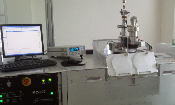
J. A. Woollam VUV-NIR spectroscopic ellipsometer equipped with UHV cryostat (spectral range 0.75- 9 eV / 1700 nm-148 nm, temperature range 5 – 1000 K). This system allows measurements in NIR- VUV range in vacuum or dry nitrogen atmosphere.

Contact:
Alexandr Dejnekadejneka@fzu.cz
In situ ellipsometry refers to dynamic measurements during the modification process of a sample. This process can be, for instance, the growth of a thin film,etching or cleaning of a sample. By in situ ellipsometry measurements it is possible to determine fundamental process parameters, such as, growth or etch rates, variation of optical properties with time.

- Ellipsometer J.A. Woollam, M2000
- Incident angle 76.5°
- Spectral range: 245-1700nm
- Sampling rate: 1Hz or 10Hz
Contact:
Jiří Bulířbulir@fzu.cz
Infrared ellipsometry
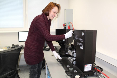
In the infrared region of the spectrum, it is possible to analyze primarily the phonon vibrations of the crystal grid and electro-transport properties characterized by the concentration of free charge carriers and their mobility. In case of non-uniform or gradient depth profile of the sample under study, it can be even distinguished between the surface and bulk conductivity, or to determine the concentration profile of free charge carriers from the sample surface towards its volume.

Spectrophotometry
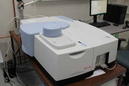
Laboratory of spectrophotometry is equipped with spectrophotometer PerkinElmer Lambda 1050 with Optical cryostat

| Lambda 1050 | |
| Wavelength Range | 175 – 3300 nm |
| UV/Vis Resolution | ≤ 0.05 nm |
| NIR Resolution | ≤ 0.20 nm |
| Photometric Range |
8 A ( Vis / NIR) No additional Attenuation required |
| Photomultiplier Detector (UV/Vis) | R6872 gridless |
| NIR Detector |
Peltier cooled InGaAs (-50°c) 860-1800nm / 860-2500nm Peltier-controlled Pbs 860-3300nm |
| Sample and Reference Beam Attenuators | 1%, 0.1% standard |
Contact:
Jiří Bulířbulir@fzu.cz
Optical Lithography
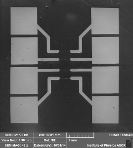
The laboratory of optical lithography was equipped (in June 2014) with the optical lithograph Microwriter ML from the Lot Oriel company with direct writing with 16 UV lasers emitting at the wavelength of 405 nm with a maximum resolution of created structures of 0,6 micrometers. The lithograph has an automatic adjustment of the samples to the focus of the lasers. Optical lithography, together with a system for the preparation of photoresists and chemical laboratories for subsequent etching (plasmatic by Reactive ion etching, or chemical), will form the basis of a new laboratory for the preparation of micron structures.


Contact:
Ján Lančoklancok@fzu.cz