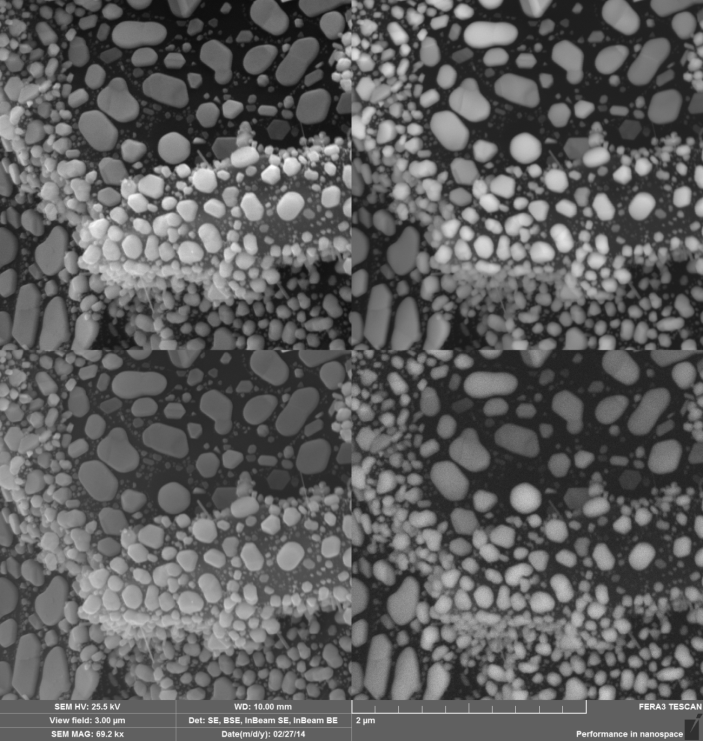
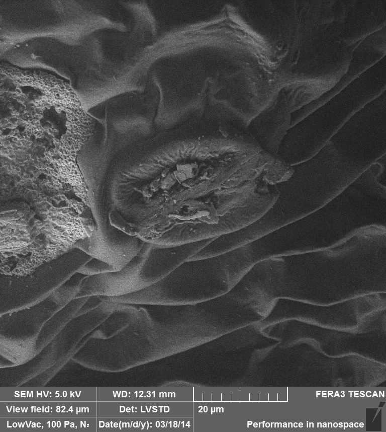
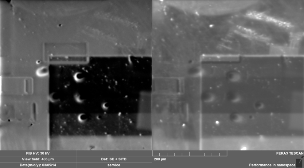
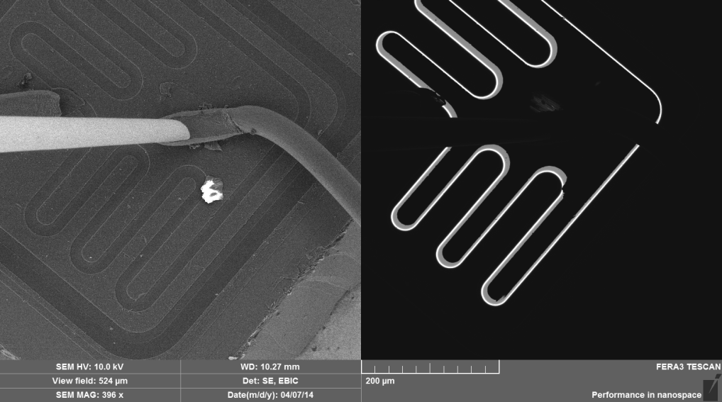
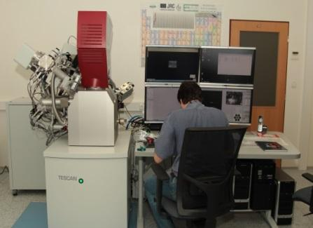
The scanning electron microscope (SEM) Tescan FERA 3 was installed at April 2014. The installed apparatus have couple of unique features, it was the first SEM with the plasma focused ion beam (FIB) installed in the academic sphere worldwide for example.
SEM is equipped with conventional secondary electron detector and motorized retractable back-scattered electron detector. The second set of detector are “in-beam” detectors for the working distances below 5 mm. Secondary electron detector allows resolution 2 nm at acceleration voltage 30 kV and 2,5 nm at 3 kV; back-scattered electrons detector have resolution 2 nm. The acceleration voltages can be exploded in the interval 1 to 30 kV. The beam deceleration mode can lower acceleration voltage of the electrons falling on sample down to 200 V. Such method – low voltage SEM – can improve imaging of less conductive samples. The non-conductive samples ca be imagined with the low vacuum SEM. The nitrogen gas up to 500 Pa can be used in our SEM, as conventional water vapor atmosphere could not be used due to the possible negative interaction with FIB in the chamber. The resolution of the special Tescan low-vacuum secondary electron detector is 2 nm at 30 kV and 3,5 nm at 3 kV at least.
The xenon plasma FIB allows imaging of the surfaces and micromanipulation. The acceleration voltages are within the range 3 to 30 kV. Due to the technology used the maximum current can reach 2 A. The secondary ions detector offers the possibility to imagine surface not only with the electrons. The ion beam digs the trenches – cross-cuts and prepare lamellas with the use of nanomanipulator. The gas injection system (GIS) with five gases can be used for surface modification or coverage. There can be deposited platinum, tungsten or silicon oxide and modification of silicon or photoresist can be done with water and fluorine XeF 2 gas. The inspection of thin samples can be performed in scanning transmission electron detector (STEM).
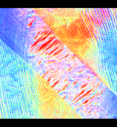
There is wide set of analyzers installed. The detector EDAX Octane Super with the active area 60 mm 2 allows energy-dispersive spectroscopy (EDS). The EDAX Digiview 4 analyzer can be used for electron back-scattered diffraction method (EBSD). Both analyzers can work together using so called CHI scan technique. The cathodoluminiscence signal is detected by four-channel detector produced by Tescan. The SEM producers provide the electron beam induced current measuring system as well.
The construction of 3D tomography is possible in all detection modes and all analyzers thanks to the FIB and dedicated software of both SEM and analyzers producers and ORS.
The giant chamber of SEM is used not only for sample´s mounting, but can be exploited for the functional stages too. The STEM detector was already mentioned. Except that the Peltier stage can be mounted and samples heated up to the 70 °C or down to the -50 °C. The deformation stage Gatan Mtest2000 with jaws for EBSD applies stress in tension or pressure up to 2 kN.
The significant amount of work was already published after more than two years of work in FUNBIO SEM laboratory including majority of presented techniques.
